
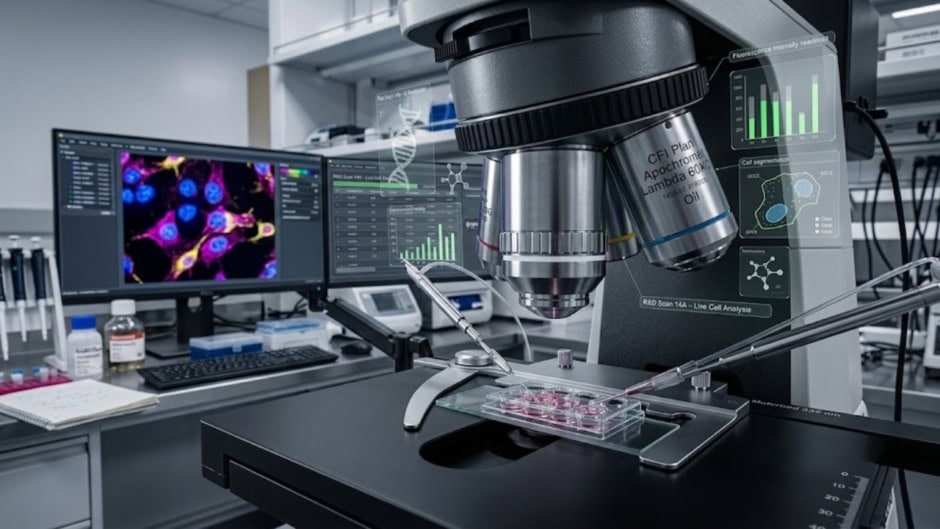
The US Department of Energy’s Brookhaven National Laboratory installed a custom-built electron microscope that represents a fundamental leap forward in materials science research.
The scanning transmission electron microscope at the Center for Functional Nanomaterials delivers energy resolution 200 times sharper than existing instruments. It enables scientists to examine atomic structure, chemical composition, and electronic behavior simultaneously.
The breakthrough matters because understanding how materials behave at the atomic scale directly translates to better batteries, faster semiconductors, and advances in quantum computing. Previous microscopes forced researchers to make tradeoffs. A scientist studying a battery cathode material could examine its structure or its chemistry, but not both together in real time. This instrument eliminates that limitation.

Four major technological advances power the new capability. A pair of secondary electron detectors can simultaneously image the top and bottom surfaces of a sample with atomic precision. This dual-surface imaging proves invaluable for catalyst research because catalysts drive the chemical reactions inside batteries and fuel cells. By watching both surfaces before and after a reaction occurs, researchers can now understand exactly how catalyst structure changes during operation.
“Even the most advanced X-ray imaging techniques are generally limited to spatial resolutions on the scale of tens of nanometers, whereas modern electron microscopes can provide atomic-scale information,” said Sooyeon Hwang, who made significant contributions to the acquisition of the microscope and was a scientist in CFN’s Electron Microscopy group at the time. She is now an associate professor at Dongguk University.
The microscope’s energy filtering system achieves that remarkable 200-fold improvement by employing momentum-resolved electron energy-loss spectroscopy. This technique allows scientists to evaluate quasiparticles like phonons, magnons, and plasmons. These exotic entities govern how materials conduct heat, respond to magnetic fields, and interact with electricity and light. Previously unobservable behavior now becomes visible.
Operating at voltages as low as 20 kiloelectron-volts, compared to the typical 100 to 300 keV range, the microscope minimizes damage to extremely delicate materials. This proves especially critical for studying two-dimensional quantum materials only a few atoms thick. Lower voltage means higher scattering power and better preservation of sample integrity during observation.
Python-based software enables remote operation, opening possibilities for autonomous and machine-learning-assisted microscopy. Scientists worldwide can conduct experiments without traveling to Brookhaven. This capability could accelerate research cycles significantly.
Yimei Zhu, senior physicist leading Brookhaven’s advanced electron microscopy group, emphasized that the instrument pushes the current limits of microscope instrumentation.
“We have really pushed the current microscope instrumentation limit,” Zhu said. “This voltage is particularly designed for two-dimensional quantum materials, which are often one or a few atomic layers thick. Lower voltage electrons not only have higher scattering power but also can minimize damage to sensitive materials.”
“With [this] new instrument, we are now able to feel more of the elephant,” Yang added. “We can finally get at the truth, what’s really there, and I think that’s pretty exciting. It’s what we all want to do as scientists.”